MIDs Make A Comeback
3D molded interconnect devices were supposed to be the 1980s' breakthrough for plastics in electronics—but they flopped. New processes that make market entry faster, simpler, and less costly have recharged MIDs' prospects.
Back in the 1980s, 3D molded interconnect devices (MIDs) were hailed as a breakthrough in electronics. They were expected to eliminate conventional circuit boards by putting conductive paths directly onto the surface of molded plastic devices. After failing to meet those exuberant expectations, 3D MIDs are gaining broader acceptance today as new processes, materials, and technologies converge to better meet the demands of circuit-carrying plastic parts.
Many industry observers believe MIDs have finally come of age. The market is experiencing annual growth of about 20%, according to the Research Association Molded Interconnect Devices (3D-MID) in Erlangen, Germany. The driving forces are miniaturization, tighter electronic packaging, and increased functional demands. To meet these new requirements, new processes such as laser direct structuring (LDS) and "flex foil" film-insert overmolding have emerged as ways to simplify MID production, reduce cost, and speed product development. In tandem, material suppliers are working to develop plateable and non-plateable grades that have good adhesion, dielectric properties, and high-temperature resistance for growing MID markets like automotive electronics, telecommunications, and medical devices.
A rocky start
When MIDs were born almost 20 years ago, the prospect of producing injection molded circuitry carriers was greeted with huge fanfare. Engineering-resin makers rushed out new materials and innovative processes and formed partnerships with MID producers in a headlong drive to crack what was believed to be a multi-billion-dollar market potential.
The reasons for the disappointing results are varied but most agree that the technology available back then was too complex and costly for most users. Its lack of flexibility and speed to market were also limiting factors. Many companies investigated the new MID technology but most pulled back because of high development cost, according to Nils Heininger, product manager at LPKF Laser and Electronics AG in Garbsen, Germany, the developer of a promising new laser-based MID process.
"The one thing all the processes had in common at the time was use of tooling specific to a particular circuit layout, which made it difficult for prototyping, design changes, and producing smaller volumes," says Heininger.
Another obstacle to mass commercialization was the lack of a unified network or infrastructure to support and produce MID parts. "It was hard to push because MIDs were a totally different concept," says Alexander Radeck, application development engineer for resin maker Lanxess (a recent Bayer spinoff) in Germany. "The guys working on the electrical side had nothing to do with the plastics people and you needed to bring all of them together at one table."
Moreover, some observers believe that the MID know-how was concentrated among too few companies. "Not many parties had the full capabilities to produce MIDs," explains Andreas Kunze, executive secretary of the 3D-MID Research Association. "There were groups that metallized, those that structured, the molding people, and very few that knew all facets." Overall, electrical/electronic manufacturers were averse to taking a risk on a new technology that was burdened by several market-entry restrictions.
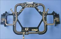
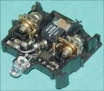
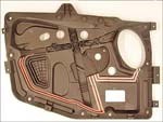
The most important attribute of MIDs is their ability to reduce the number of components in an E/E product. For example, circuit paths can be integrated into a plastic housing as a substitute for a conventional printed circuit board. By uniting electrical and mechanical functions in a single unit, MIDs bring huge advantages in manufacturing and assembly. MIDS can provide 3D circuitry arrangements, whereas conventional PCBs are typically limited to 2D planes. MIDs can reduce component count and cost by integrating features such connectors, sockets, or other devices.
Despite MIDs' well-documented advantages, many E/E design engineers still think in 2D and MIDs only make sense in a 3D framework. "The aim is not to replace an existing part but create a new one," explains Ticona product development engineer Tobias Schuler.
Tried-and-true processes
Today, two-shot molding and hot stamping are the two most widely used MID processes. Two-shot molding produces MIDs from a combination of plateable and non-plateable injection molded resins. A plateable polymer is molded in the first shot and is then selectively overmolded with a second non-plateable material, leaving some areas of the first material exposed. An etching step then activates the exposed areas of plateable polymer so that those areas can be plated with a metal such as copper.
In hot stamping, a special metal foil is placed in a heated die and the circuit layout is transferred to a molded part.
Both processes can use a range of materials from ABS and PC to nylon, PBT, PPS, and LCP. LCPs are widely used in small parts and two-shot components that require high flow and high heat resistance to withstand soldering of electronic connections to the MID circuitry.
Both two-shot molding and hot stamping have drawbacks that limit their use. Two-shot has high initial tooling costs, which many believe limit its use mostly to higher volume applications. The process also has limited design flexibility, limited prototyping ability, and long development times. Hot stamping has lower development and tooling costs but is suitable mainly for simpler and larger parts with limited geometry (only 2D layouts on 3D parts).
Laser delivers simplicity
Among the newer MID processes that have emerged to fill in the gaps in cost, flexibility, and part complexity, one that is attracting the most attention is the laser direct structuring (LDS) process from LPKF. The system uses a laser to "draw" a circuit on the surface of a part molded containing a laser-sensitive additive. The process is claimed to be simpler than conventional methods and is more environmentally friendly because it eliminates chemical pretreatment (e.g. etching) during the metallization step.
At the heart of the process is a plastic compounded with a special laser-sensitive metal complex developed by LPKF. When the polymer is exposed to the laser, the metal complex is broken down into elemental metal—either copper or palladium—and residual organic groups. The laser draws the circuit pattern onto the part and leaves behind a roughened surface containing embedded metal particles. These particles act as nuclei for the crystal growth during subsequent plating with copper.
The LDS process involves three main steps: injection molding, laser structuring, and electroless plating. Since it uses a single material, it offers much lower tooling and equipment cost and complexity than two-shot molding. In addition, LDS accommodates ultra-fine circuitry—down to 250 microns wide, vs. a minimum of 400 microns for two-shot molding and 1 mm (1000 microns) for hot stamping.
Unlike other MID processes, LDS is very flexible because circuit designs can be modified simply by reprogramming the laser unit. "It's a flexible process that stores the circuit design in the computer," says LPKF's Heininger. "There's no worry over costly and time-consuming tool or die changes." Another advantage is that the laser also performs the plastic surface preparation, unlike two-shot molding, which requires an additional etching step to prepare the plastic for plating.
Heininger views LDS as a breakthrough technology that will bring more users into the MID fold. Others say LDS will give users more trust in the MID technology because of its prototyping capability and flexibility. For example, a potential user could ramp up a new product in LDS and then possibly switch to a two-shot process if volumes increase sufficiently.
Special LDS resin grades
LPKF has worked with several engineering resin companies such as BASF, Degussa, Lanxess, and Ticona to develop material formulations for the LDS process. These materials so far have included nylon, PBT, and LCP, but LPKF is anticipating additional materials such as PC/ABS.
Ticona is already actively in volved in two-shot molded MIDs and is making a big push in LDS. For two-shot molding, Ticona offers Vectra E820i Pd, a 40% mineral-filled LCP with palladium as the plating catalyst. Applications include high-frequency connectors, auto sunlight sensors, cell-phone antennas, and electrical devices for digital cameras.
For LDS, Ticona has developed Vectra E820i LDS, a 40% mineral-filled LCP with a melting point of 340 C and HDT of 225 C. LCP's high flow and heat resistance make it a strong candidate for MIDs that require reflow soldering. "The time is ripe for LDS technology because it is allowing MIDs to realize their potential," says Ticona's Schuler.
Ticona worked with MID maker Harting Mitronics in Biel, Switzerland, to develop the first commercial LDS application made of LCP. This MID for Siemens' Acuris P hearing aid uses Vectra E820i LDS. Other LDS development projects are focused on sensors, connectors, antennas, and security applications. Ticona is also developing a higher-heat grade, Vectra S, with an HDT of 340 C for applications like LED lighting. For new "flip chip" technology, Ticona is working on grades with improved coefficient of linear thermal expansion. In these advanced applications where silicon chips are placed directly on the circuit, the molded carrier must have high dimensional stability and low variation under a range of thermal conditions, according to Schuler. These new materials with CLTEs of 15 to 20 ppm are expected to be commercialized by the year's end. Micropackaging applications such as sensor packages, antennas, connectors, and hearing aids are targeted.
Meanwhile, Lanxess has developed three new Pocan TP polyester grades with a wide processing window for LDS. High-heat Pocan TP710-004 is a 40% glass- and mineral-filled PET/PBT blend with an HDT of 250 C. This makes it suitable for both reflow and vapor-phase soldering and also lead-free soldering. Pocan DP7102 is a 25% mineral-filled PBT with good flow and a melting point of 225 C. And Pocan TP 710-003 is a PBT developed for extruded profiles. These materials are claimed to provide low moisture absorption, high stiffness at high temperature, dimensional stability, and good dielectric properties over a broad temperature range.
Lanxess is also developing grades that are flame retardant and have lower CLTE. The company has two commercial LDS-MID applications in security housings. Another key target is automotive, where switches, sensors, and activators are being investigated.
Degussa AG in Germany has developed a crosslinkable PBT for LDS that offers short-term heat resistance up to 340 C. Vestodur CL2230 is a 30% glass-filled grade described as a cost-effective alternative to high-heat polymers like LCP. The modified PBT is crosslinked with beta or gamma radiation at the end of the electroplating process, making it suitable for lead-free soldering. Degussa is nearing commercialization of two applications: a micro antenna and an auto steering device. The company also offers crosslinkable PBT grades for two-shot molding, such as non-plateable Vestodur CL2030 and plateable Vestodur CL2120 with an iron-based catalyst.
BASF developed Ultramid T KR4380 LS, a semi-aromatic nylon 6/6T with 30% glass, for the LDS process. With a melting point of 295 C and HDT of 270 C under load (285 C with no load), it meets soldering requirements. Other variants, like low-warpage grades with glass/mineral reinforcement, are in development. BASF has not landed a commercial application but is focused on low-amperage automotive applications such as sensors, switches, and air-bag components.
One-step automation
Another innovative MID process is the "flex foil" film-insert overmolding technology developed by injection molder and moldmaker Erwin Quarder Werkzeugbau GmbH of Espelkamp, Germany. The three-year-old process patented by Quarder and film producer Freudenberg Mektec Europa GmbH of Weinheim, Germany, is claimed to be the only fully automated process for MID manufacturing.
The one-step process starts with a 0.3-mm-thick flexible film consisting of a copper layer with circuit paths between two sheets of polyimide. Freudenberg Mektec (or Mektec International in the U.S.) ships the films in trays. After predrying the film in an oven, a three-axis robot positions it in a flat fixture. A five-axis robot then places the film in the injection press for overmolding. The automated process also includes soldering of microswitches and a final quality test. A 30% glass filled PBT is typically used for the backing resin. The polyimide foil withstands temperature peaks of 310 C and continuous temperatures of 150 C.
Quarder is using its foils to produce MID door-locking systems for a European car maker at a rate of 2.9 million parts/yr. Nineteen different versions of the locking system are being made on four production lines.
Metal spraying & printing
Another new process uses a metal-spraying technique to manufacture MIDs with thicker circuitry (200 microns on up). The FlameCon system from Leoni AG, a German wire and cable producer, is used after laser structuring roughens the plastic surface for good metal adhesion in the areas where circuit paths are to be deposited. One advantage is that plateable plastics are not required. The technique is also free of chemical processes and less costly than most MID manufacturing methods, according to Knuth Gotz, acting head of central R&D at Leoni. It is currently unsuitable for fine-pitch MIDs but Leoni is working on components with 200-micron pitch.
Leoni developed the process using metal-spraying technology from an existing commercial supplier. However, Leoni expects to produce its own equipment for next-generation systems. Leoni has experimented with the process on plastics ranging from polystyrene to PEEK, but most applications in automotive and toys are currently focused on nylon, PP, or ABS. The company wants to license the technology in the U.S. and Europe.
Primer technology offered by Austrian MID manufacturer I&T (Innovation & Technology) and its partners, Tier I auto supplier Magna International and 3M, makes it possible to deposit circuit layouts by screen printing on film substrates using a plateable primer. I&T acquired the so-called Baymetec technology from Bayer MaterialScience two years ago. The polyurethane-based primer ink, which contains a catalyst for copper plating, is screen printed on film of PET, PEN, PC, PC blends, or PEI (GE's Ultem). After the ink is dry, the film is placed in an injection mold and overmolded with a non-plateable ABS, PC, or blend. Then the part is copper plated in a chemical bath.
While the flexible film permits easy application of metal conductive paths, the process is limited by the thinness of the printed conductive paths. At only 3 to 5 microns, these circuits are suitable for low-amperage applications. No commercial uses have surfaced yet, though I&T has several developmental projects, mostly in low-current auto sensors.
Two-shot holds its own
While LDS and film insert molding have attracted much attention lately, older MID processes like two-shot molding remain viable, especially with new enhancements. Tyco Electronics, Rochester, N.Y., acquired the former MID LLC in 2001 and has successfully applied two-shot technology in high-volume MID applications. According to product manager Max Leone, Tyco developed unique tooling and processing techniques that make two-shot molding repeatable and cost-effective.
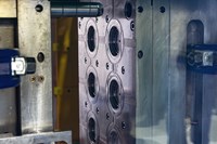
Tyco's solution to this method's previous drawbacks—complexity and inflexibility—include "universal" mold designs that incorporate inserts for different MID products, saving changeover time and reducing cost. Leone also says that advances in hot-runner nozzles have boosted reliability and enabled molding machines to run longer and make more complex components. A big business for Tyco is internal antennas for cell phones that are two-shot molded with a range of materials, including syndiotactic PS (until Dow's recent pullout) and ABS. The company is also exploring plastic/metal hybrid MIDs that would incorporate a metal stamping in the mold or in a secondary press-fit operation.
Meanwhile, DuPont Engineering Polymers has developed a plateable LCP doped with palladium catalyst for two-shot molding. Zenite 55801 is based on the Titan 5000 LCP chemistry that DuPont acquired from Eastman Chemical. It is a high-flow material with an HDT of 275 C to withstand lead-free soldering. MIDs for hand-held consumer electronics are a target, according to Bill Hassink, DuPont's connector industry manager.
Multi-process competency
In order to foster the growth of MID applications, a growing number of MID producers have expanded their capabilities to include multiple MID manufacturing processes. An example is Harting Mitronics in Switzerland, one of the world's largest connector makers. It produces MIDs via two-shot molding and LDS. "Two years ago, we decided that someone must stand up and industrialize this business and take a look at it from a customer's point of view," explains Jorg Hehlgans, director of marketing and sales. Previously, interested OEM companies had to go to several parties to obtain MIDs. "But we integrated all aspects to produce the full process chain," Hehlgans says.
Similarly, Schaal Oberflaechen Systeme Komponenten in Germany is extending its competency beyond electroplating to include two-shot molding and LDS. "The company that integrates the most process technologies will have the best chance to establish a footing in the MID market," says Harald Orschel, Schaal development manager. The company's first commercial application is a security housing made by LDS of Lanxess' Pocan DP7102, a 25% mineral-filled grade. Development work is aimed at automotive switches and sensors
Related Content
How to Optimize Injection Molding of PHA and PHA/PLA Blends
Here are processing guidelines aimed at both getting the PHA resin into the process without degrading it, and reducing residence time at melt temperatures.
Read MoreMedical Molder, Moldmaker Embraces Continuous Improvement
True to the adjective in its name, Dynamic Group has been characterized by constant change, activity and progress over its nearly five decades as a medical molder and moldmaker.
Read MoreWhat to Look for in High-Speed Automation for Pipette Production
Automation is a must-have for molders of pipettes. Make sure your supplier provides assurances of throughput and output, manpower utilization, floor space consumption and payback period.
Read More‘Monomaterial’ Trend in Packaging and Beyond Will Only Thrive
In terms of sustainability measures, monomaterial structures are already making good headway and will evolve even further.
Read MoreRead Next
Beyond Prototypes: 8 Ways the Plastics Industry Is Using 3D Printing
Plastics processors are finding applications for 3D printing around the plant and across the supply chain. Here are 8 examples to look for at NPE2024.
Read MorePeople 4.0 – How to Get Buy-In from Your Staff for Industry 4.0 Systems
Implementing a production monitoring system as the foundation of a ‘smart factory’ is about integrating people with new technology as much as it is about integrating machines and computers. Here are tips from a company that has gone through the process.
Read More

.jpg;width=700;quality=80)
